EDG Reading Room
EDG Selected for gBETA Cheyenne Fall 2020
“I am grateful to announce that Engineering Design Group has been selected to participate in the gBETA Cheyenne Fall 2020 accelerator! gBETA is under the nationally ranked startup accelerator gener8tor, and has been brought to Cheyenne by Microsoft's TechSpark program.”
A note from Engineering Design Group’s founder and chief engineer, Ryan Alford:
I am grateful to announce that Engineering Design Group has been selected to participate in the gBETA Cheyenne Fall 2020 accelerator! gBETA is under the nationally ranked startup accelerator gener8tor, and has been brought to Cheyenne by Microsoft's TechSpark program. We look forward to bringing EDG's new IoT solution to market as we work alongside other Wyoming startups under guidance from our director Baylie Evans. Here's to another turn of the ratchet for EDG, and the state of Wyoming!
Together with four other startups in the gBETA Cheyenne Fall 2020 cohort, EDG will receive individualized coaching and access to gener8tor’s national network of mentors, customers, corporate partners and investors.
In EDG’s first year, our source of revenue has transitioned from contract engineering to providing a secure, customized sensor-to-smartphone solution which eliminates the barrier to IoT connectivity for our customers. The gBETA program will accelerate our ability to bring EDG’s technologies to an array of customers that need remote control and monitoring capabilities.
Documenting for Production
The contract engineer has finalized a custom PCB design for an upcoming startup. The next step is to order a run of prototypes for testing. After many months of raising capital, marketing their product, and garnering sales, the customer is in the home stretch of their first release. Once the prototypes are up and running, it will be time to scale up to a production run and fulfill the first set of orders.
The contract engineer has finalized a custom PCB design for an upcoming startup. The next step is to order a run of prototypes for testing. After many months of raising capital, marketing their product, and garnering sales, the customer is in the home stretch of their first release. Once the prototypes are up and running, it will be time to scale up to a production run and fulfill the first set of orders.
Somewhere between ordering prototype boards and delivering the tested units, the contract engineer will send a package of the finished assembly files to the startup. This file-set contains all documents pertaining to the released design. A complete assembly package allows the customer to order an exact replica of the design — resistor-for-resistor, and trace-for-trace — resulting in production assemblies that have the exact performance characteristics of the prototype assemblies.
It is imperative that the contract engineer delivers this data package to their customer with complete data integrity. This is only possible if all changes throughout the manufacturing process have been documented by engineering and relayed back to the customer. One change left out of the delivered assembly data can lead to the failure of an entire production lot.
A realistic and frequent scenario is that — after a board is placed on order — the manufacture discovers one or two parts that are no longer available through distribution. In this case, the manufacturer will propose a set of alternates to the engineer, or they will ask the engineer how to proceed. Once changes are agreed upon, it is critical that each deviation to the assembly package is rolled back to the bill of materials and the schematic, and that a revised file package is relayed to the customer. Without these key steps, data integrity is lost, and a future production run will fail to replicate the prototypes.
* * *
At Engineering Design Group, we have a background designing for mission critical applications, and we understand that high quality is directly correlated to documenting all changes prompted by the manufacturing process. Stringent documentation procedures are part of our design process whether we are developing hardware for our clients or our own secure remote monitoring products.
If your company is interested in our design expertise or learning about our quality processes, or if you would like to learn more about EDG’s secure remote integrations, contact us today.
EDG Secure Remote Integrations
Engineering Design Group, LLC announces development of secure remote monitoring products, a web-based client portal, and system integrations for Internet of Things (IoT) applications.
Laramie (Wyoming), August 10th, 2020 — Engineering Design Group, LLC announces development of secure remote monitoring products, a web-based client portal, and system integrations for Internet of Things (IoT) applications.
Data transmission from sensor to the cloud starts with an ARM Cortex R4 processor which sends data to EDG’s client portal via 802.11a/b/g/n/ac dual-band (2.4GHz and 5GHz) or LTE (Cat M1/Cat NB1/EGPRS). Global cellular connectivity is provided with an onboard SIM.
The EDG client portal provides a dashboard where customers can access data from sensors connected to arrays of their EDG systems. Sensor interfaces include I2C, SMBus, UART, and SPI, and sit alongside general purpose I/O to support a wide array of applications.
Secure data transmissions are provided through a mature third party platform and OS which provide remotely deployed security updates to the product for the lifetime of the customer service agreement with EDG.
In conjunction with the controllers, EDG will be releasing a smart battery charger with solar panel support enabling stand-alone data monitoring solutions.
EDG’s secure remote integrations can be optimized for industries such as renewable energy, natural gas, mining, and manufacturing with common applications including predictive maintenance, remote control and monitoring, asset management, and auto-replenishment. To schedule a consultation, please contact us at sales@edglab.com.
* * *
Engineering Design Group, LLC will maintain its contract engineering services as we work closely with our customers to deliver secure remote integrations for their systems. This is in alignment with our mission to help companies navigate the complex barrier of designing their own hardware, firmware, and software, so they can focus on growing their businesses.
The EDG Difference
Engineering Design Group, LLC is proud to be the first of Altium's Service Bureaus in the Equality State. But what does this mean for our clients?
Engineering Design Group, LLC is proud to be the first of Altium's Service Bureaus in the Equality State. But what does this mean for our clients?
The EDG difference. The best tools money can buy.
If your team is designing circuit boards using free EDA software, then you are simply not using the best tools for PCB design. EDG is committed to investing into our clients and our engineers. And if we can improve the signal integrity of a PCB layout in any capacity, then it justifies our investment in the best EDA software that money can buy.
That is why we’ve purchased Altium Designer, which enables EDG to be listed as a verified Altium Service Bureau.
Less time learning. More time doing.
Engineers on our team have been using Altium as their preferred EDA software since Altium Designer 6 was released in 2006. Since then, Altium has rolled out new features each year, and our engineers have been at the leading edge, incorporating these features into their designs.
Whether we are creating rules to ensure controlled impedance routing, embedding STEP models into our parts, or using Altium’s DRC to verify a sufficient clearance between ceramic capacitors and breakaway rails — our projects are designed to leverage the very best features of Altium Designer.
For our clients, an in depth understanding of Altium Designer means less time learning, and more time doing.

All About Fiducials
It’s important that the engineer or CADer who is laying out a PCB understands not just why fiducials are needed, but more specifically how fiducials aid stencil positioning and part placement during the surface-mount assembly process. A good understanding of fiducials will ensure that the PCB is designed with the correct number of fiducials, that they are properly sized, and that they are placed in optimal locations for the contract manufacturer. This attention to process during the design cycle will help eliminate errors during manufacturing.
It’s important that the engineer or CADer who is laying out a PCB understands not just why fiducials are needed, but more specifically how fiducials aid stencil positioning and part placement during the surface-mount assembly process. A good understanding of fiducials will ensure that the PCB is designed with the correct number of fiducials, that they are properly sized, and that they are placed in optimal locations for the contract manufacturer. This attention to process during the design cycle will help eliminate errors during manufacturing.
What is a Fiducial?
Fiducials are round pad markers that are placed on the PCB during the design process and are used during surface-mount assembly to aid stencil positioning and to ensure that the pick and place machine is using consistent reference points while positioning parts. A fiducial is a “no BOM” component, which means they are added to the PCB as as a component, but do not appear on the bill of materials because no component is soldered to the pad of the fiducial.
How are they used?
Fiducials are used early in the manufacturing process before any parts are soldered to the PCB.
When creating a fiducial, make sure it has an aperture on the paste layer. During stencil placement, the aperture is used to make sure the stencil is correctly aligned, but also to ensure that the stencil is placed with the correct orientation prior to solder paste application. Without having fiducials apertures on the stencil, there would be no way to align the stencil, as the stencil’s only apertures would be for components where solder paste is applied.
Once the solder paste has been applied to the component pads and the stencil is removed, the pick and place machine utilizes the locations of the fiducials to reference the coordinates for each part. With the fiducials acting as consistent reference points, the machine can adjust the PCB’s position under the pick and place nozzle, ensuring that each part is placed at the correct position.
Sizing
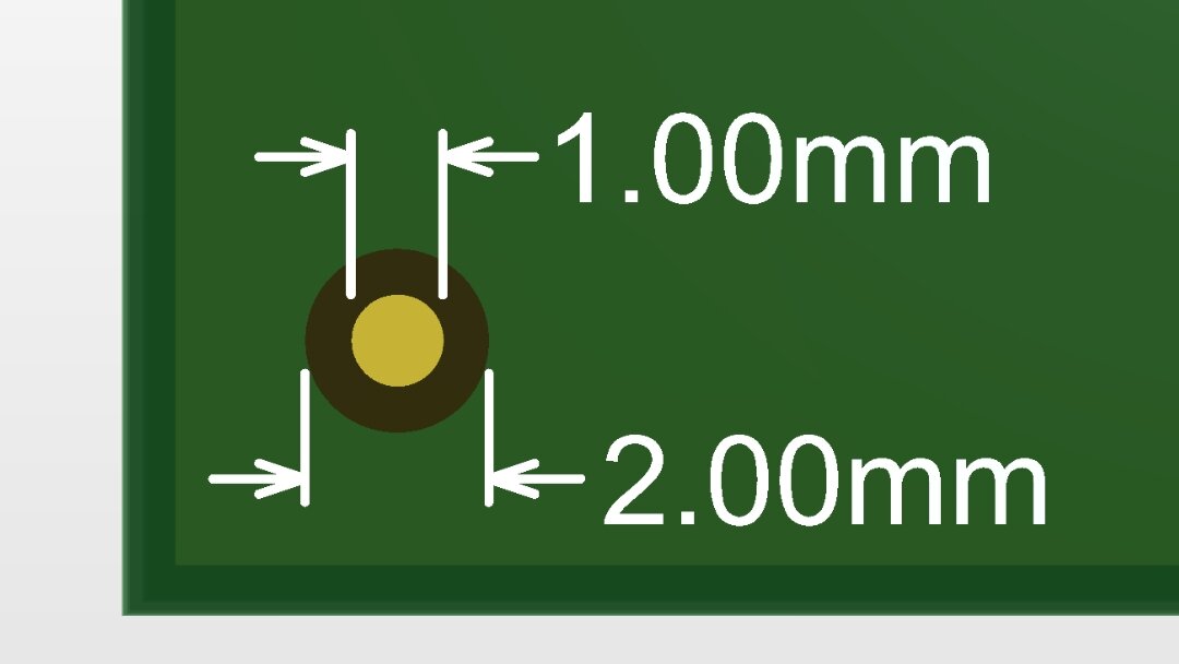
An optimal fiducial is drawn with 1mm pad diameter, and a mask backoff diameter of 2mm.
While every contract manufacture may have a slightly different sizing requirement, the golden standard seems to be a fiducial that has a 1mm diameter pad, with solder mask backed off from the center by 1mm in each direction, resulting in a 2mm solder mask circle.
The mask is backed off away from the pad to expose the rough appearance of the inner PCB material, which results in more contrast against the gold pad than if the mask were directly adjacent to to the pad. This contrast helps the machine detect the fiducial pad without discrepancy.
Quantity
While two fiducials will create an angle to verify orientation of a PCB, two fiducials per PCB are not enough. A design with parts on both sides of the board and only two fiducials can result in the PCB being inserted into the machine upside-down. In this case, the stencil would correctly align with the two fiducials, but solder paste would be applied in the wrong locations as the stencil apertures are intended for applying paste to the other side of the PCB. Four fiducials placed symmetrically with respect to each other can cause the same issue, but could also result in an incorrect rotation of the stencil, leading to invalid solder paste application.
A quantity of three fiducials is the perfect number to eliminate accidental misplacement of the stencil with respect to the PCB.
Locations
Generally, fiducials are placed on the frame or rail edges of a PCB, which are held by the pick and place machine as the board is rolled down the conveyor belt. The fiducials should be placed such that they are not blocked by the machine where it holds onto the rails. Similarly, they should be placed with sufficient clearance from the frame or rail edges, and away from any mounting holes, pads, traces, or silk screen which may be nearby.
The fiducials should be positioned such that the intersecting line between a pair of fiducials along one edge are parallel or at a right angle to the PCB edge. (Or for the case of non-square boards, parallel or right angle to the direction the PCB will travel through the pick and place machine). When possible, the distance between a pair of fiducials measured along one side of the PCB should be different from the distance between the pair of fiducials measured along the length which is perpendicular to the first pair.
Fiducials should be placed on the top and bottom of the PCB so that the bottom-side fiducials are directly across from the top-side fiducials. This in conjunction with positioning the fiducial pairs at different distances will help catch a PCB which has been inserted into the machine upside-down. To eliminate any opportunity for offsetting the fiducial pads between the top and bottom sides of the board, I like to draw my fiducial footprints such that one footprint contains the pads, paste apertures, and proper mask backoff for fiducials on both the top and bottom side of the PCB.
To ensure the best locations of your fiducials, talk to your contract manufacturer before ordering the PCB.
Global vs. Local Fiducials
The fiducials we’ve described thus far are referred to are “Global Fiducials”. However, there are also similar positioning references known as “Local Fiducials”. On large boards that have components with dense pin grids and tight pin pitches, placing a local fiducial near the corner of the component may help the CM ensure that the part is correctly aligned. These should not be placed without first consulting your CM. On smaller PCBs where global fiducials are relatively near any component, it is unlikely that local fiducials are necessary.
* * *
When you are working in tandem with the same contract manufacturer for multiple projects, any special requirements they may have regarding fiducial sizing and positioning will become apparent after working together on your first design. However, fiducial sizing and positioning for one CM may not be convenient for another. When working with a new CM, we recommend contacting them during the PCB layout process to give them an opportunity to provide any feedback on your design.
Designing an IoT Device?
Connect it to the EDG Client Portal:
Reap the benefits of secure IoT data retention without building the infrastructure from the bottom-up
Read, calibrate, and command fleets of devices
Make IoT data available to customers, team members, and partners
Unify how developers access device data – regardless of manufacturer – without diving into low-level embedded code.